
Professor of Materials Science
MEng University of Oxford
DPhil University of Oxford
Prof Rachel Oliver has benefitted from the University's policies on flexible working, in line with the Department's commitments to the Athena Swan Charter. She was interviewed about her experiences by Chemistry World.
The Cambridge Centre for Gallium Nitride
As Director of the Cambridge Centre for Gallium Nitride, Prof Oliver’s research interests focus on the characterization and exploitation of nanoscale structures in GaN-based materials. The broad aim of my work is to achieve improved performance in GaN-based electronic and optoelectronic devices and to develop and implement novel device concepts.
Cambridge is also the main supplier of nitride epitaxy in the EPSRC National Epitaxy Facility (NEF), and provides nitride materials to academics across the UK (https://www.nationalepitaxyfacility.co.uk/).
Nitride optoelectronic devices
The semiconducting nitrides are a key optoelectronic material, which enabled the development of energy efficient light bulbs based on light emitting diodes (LEDs). Whilst the blue LEDs use in such light bulbs are a tremendously successful technology, nitride LEDs at other wavelengths – from the red to the ultra-violet – suffer from low efficiencies. Hence, our research on LEDs focusses on the links between the structure of the nitride materials and the performance of the devices, and how the structure – particularly of the active, light emitting region – can be engineered to improve efficiency.
However, research on nitride optoelectronics extends far beyond the humble LED, and increasingly encompasses exotic devices such as single photon sources. Early single-photon sources emitting in the visible spectral region were based on heavy attenuation of a laser; such sources are intrinsically unreliable, and may emit multiple photons. In contrast, we aim to build a single-photon source, based on InGaN quantum dots, that is reliable and easy to operate. Such a device would find broad application in quantum cryptography and quantum computing, particularly as the emission wavelength of the InGaN dots is rather convenient in terms of available detectors. However, the high defect density and unusual electrical properties of GaN make realising the device a challenge.
Nitride electronic devices
Nitride transistors are increasingly used in high frequency, high voltage, high temperature and high efficiency applications. In the control and conversion of electric power, silicon-based devices are no longer able to meet the demands of industry. However, GaN can endure greater electric fields than silicon, and GaN-based devices can be made with lower resistances. Whilst the nitrides have superior materials properties, they are a much less mature materials system than Si. Typical nitride transistors have very high densities of defects, and one of our research foci is understanding the impact of these defects on device performance. We are also interested in developing crystal growth routes which allow improved heat dissipation from nitride devices, and which enable new or enhanced device functionality.
Novel Nitride Materials
GaN in its stable wurtzite crystal structure has achieved amazing things in both electronics and optoelectronics. However, the alternative metastable zincblende structure may offer solutions to some of the enduring problems of nitride technology, such as the relatively low efficiency of red, green and amber nitride LEDs. This is because the zincblende structure can be used to avoid internal electric fields which arise as a consequence of the low symmetry of wurtzite crystals and degrade the efficiency of wurtzite light emitters.
Zincblende GaN is just one of the novel nitrides studied in the Cambridge Centre for Gallium Nitride. We have also developed new technologies for the fabrication of porous nitride materials, and Prof Oliver is Chief Scientific Officer of related spinout company Poro Technologies. As well as investigating and exploiting the novel properties of porous GaN, we are interested in infiltrating dissimilar materials into the pores in order to create composites with new properties, opening paths to new applications.
Development of characterisation techniques for nitride semiconductors
To improve the performance of GaN-based devices we need to understand their structure and electronic properties on a micro- to nano-metre scale. New techniques are being developed to meet the demands of this unusual semiconductor. An ongoing approach, pioneered by the Cambridge Centre for Gallium Nitride is to combine multiple microscopy techniques all focussed on the same defect or nanostructure in a nitride device. The microscopes applied range from techniques commonly used on metals (such as atom-probe tomography) to techniques which focus exclusively on semiconductors (such as scanning capacitance microscopy). Recently, we have added time-resolved cathodoluminescence to the suite of applicable techniques, allowing us to relate the structure of nitride materials to the mechanisms by which nitride devices operate. Overall, the aim is to provide a more complete picture of nitride materials science than has previously been achieved, and to apply this new understanding to engineering improved materials for nitride optoelectronic devices.
| Porous GaN structures can be formed by electrochemical etching, generating a flower-like pattern of pores which is observed in transmission electron microcopy. Zooming in on the centre of the flower, atomic resolution imaging reveals a defect, known as a threading dislocation from which the pores radiate. Understanding this detailed nanoscale structure allows us to understand the optical properties of porous GaN. | 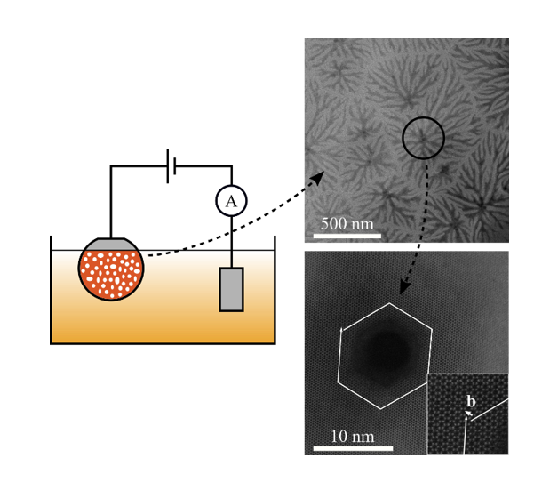 |
- Massabuau, F. C.-P.; Griffin, P. H.; Springbett, H. P.; Liu, Y.; Kumar, R. V.; Zhu, T.; Oliver, R. A. "Dislocations as channels for the fabrication of sub-surface porous GaN by electrochemical etching", APL Materials, 8, (2020) 031115, DOI: 10.1063/1.5142491
- Lee, L. Y.; Frentrup, M.; Vacek, P.; Kappers, M. J.; Wallis, D. J.; Oliver, R. A., "Investigation of stacking faults in MOVPE-grown zincblende GaN by XRD and TEM", J. Appl. Phys., 125, (2019) 105303, DOI: 10.1063/1.5082846
- Lim, K. T. P.; Deakin, C.; Ding, B. N.; Bai, X. Y.; Griffin, P.; Zhu, T. T.; Oliver, R. A.; Credgington, D., "Encapsulation of methylammonium lead bromide perovskite in nanoporous GaN", APL Materials, 7, (2019) 021107, DOI: 10.1063/1.5083037
- Wang, T.; Puchtler, T. J.; Zhu, T.; Jarman, J. C.; Nuttall, L. P.; Oliver, R. A.; Taylor, R. A. , "Polarisation-controlled single photon emission at high temperatures from InGaN quantum dots", Nanoscale, 9, (2017) 9421-9427, DOI: 10.1039/c7nr03391e
- Zhu, T.; Liu, Y.; Ding, T.; Fu, W. Y.; Jarman, J.; Ren, C. X.; Kumar, R. V.; Oliver, R. A., "Wafer-scale Fabrication of Non-Polar Mesoporous GaN Distributed Bragg Reflectors via Electrochemical Porosification", Scientific Reports, 7, (2017) 45344, DOI: 10.1038/srep45344
- Massabuau, F. C-P.; Rhode, S. L.; Horton, M. K.; O'Hanlon, T. J.; Kovacs, A.; Zielinski, M. S.; Kappers, M. J.; Dunin-Borkowski, R. E.; Humphreys, C. J.; Oliver, R. A. , "Dislocations in AlGaN: Core Structure, Atom Segregation, and Optical Properties", Nano Letters, 17, (2017) 4846-4852, DOI: 10.1021/acs.nanolett.7b0169