


![]()
We conduct world leading research into nitride based III-V semiconductors: material quality, characterisation and device development.
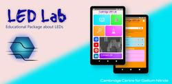
We are passionate about education and outreach! If you would like support for an education project then please get in touch.


© 2024 University of Cambridge