The innovative characterisation challenge area focuses on the development of techniques to study the properties of materials in novel ways, and extract quantitative information from imaging, spectroscopy and diffraction data. X-ray scattering, scanning probe and electron microscopy play a fundamental role in this area, while theory and modelling are essential in the design of experiments and interpretation of the results.
Our vision is to test and capture the behaviour of materials under realistic working conditions, from the micron to atomic scale, with the aim of optimising processes and developing new functionality.
New techniques enable imaging of plastic flow in brittle materials, strain measurements in small-scale tests, 3D nanoscale imaging across a range of materials, in-situ electron microscopy of composite nanomaterials, neutron and X-ray scattering of sctructural materials. Applications include high toughness ceramics, scaffolds for tissue engineering, superalloys, polymers, catalysts, energy harvesting and energy storage devices.

X-ray microtomography offers a method of evaluating, non-destructively, the structure of three dimensional biomedical scaffolds and drug delivery systems in different dosage forms. The technique provides detailed information about the nature of porosity in structures ranging from ceramic powders, through drugs and excipients to macromolecular scaffolds. In particular, by controlling the dimensions of fenestrations between the pores in tissue engineering scaffolds, it is possible to determine cell migration - producing a “cellular sieving” effect through structural
control. (cube side 1 mm).
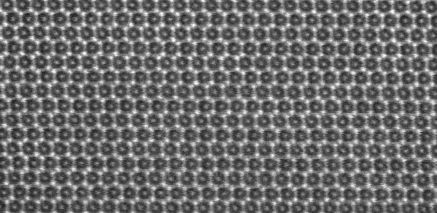
The introduction of lenses with aberration correction has led to new insights into the structure of modern materials. The atomic arrangement can now be realised in STEM images with sub-Ångström resolution, with high clarity and with straightforward interpretation. The example of heavier Ta and lighter Cr atomic columns is shown in the Figure.


The remarkable versatility of modern electron microscopes enables the 3D structure and composition of nanoscale materials and devices to be determined by modern electron tomography.
Incorporating analytical techniques such as electron energy loss spectroscopy enables 3D optical and electronic information to be determined and by combining with diffraction a full 3D crystallographic analysis is possible.
The exquisite sensitivity of the electron beam to the crystal potential and thus atom positions, lattice vibration and possible phase transitions makes it an ideal probe to study crystallography with nm spatial resolution. A variety of materials are being investigated including polyethylene, MOFs, zeolites, pharmaceutical crystals, superalloys and carbon nitride.


Dynamic processes can be studied in situ in the electron microscope, under operating conditions compatible with a range of processes. Research includes battery electrodes and charge-discharge cycles, electroless plating and corrosion, caloric and piezoelectric composites, metal-oxide catalytic interactions under controlled gaseous environments. The Wolfson Electron Microscopy Suite is equipped with state of the art FIB, SEMs, and TEMs as well as specimen holders for in situ experiments.
The optimal use of structural materials requires a detailed understanding of the mechanistic origins of their behaviour in service. This is acquired using international neutron and synchrotron X-ray radiation sources equipped with a range of scattering techniques. Measurements are also performed in situ, at service representative conditions, including under applied stress and elevated temperature.

Multi-microscopy (Oliver)

Atomic force microscopy was originally envisaged as a technique for measuring nanoscale surface topography. Today, we not only use it to address the electrical properties of materials at the nanoscale, but combine it with other techniques, such as electron microscopies, to relate the electrical properties of a specific nanostructure to the optical properties, the defect structure of the material and its composition.
Microstrain and plasticity in brittle materials
There is an extensive interest in understanding how brittle materials plastically deform. Direct measurement of yield stresses over a wide range of temperatures, combined with extensive computation, is leading to the discovery of completely new strategies for developing toughness in materials.
A major difficulty in small-scale tests is accurately knowing the strains and deformations which the sample has undergone. For the first time, high resolution methods have been demonstrated for mapping the full strain in small-scale test samples using digital image correlation over areas as small as 0.08 x 0.08 μm2.

Small-angle scattering (light/x-rays/neutrons) (Evans)
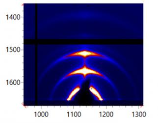
Small-angle scattering methods enable the characterisation of the structural organisation and conformation of soft materials (e.g. surfactants, polymers, colloids, gels) in solution and thin films across length scales of ~1-100 nm. Experiments are performed in-house at international large scale synchrotron and neutron reactor sources. The figure shows the 2D detector image obtained from grazing-incidence wide-angle X-ray scattering (GiWAXS) analysis of a self-assembled polymer-surfactant thin film.