Banner image: At work in the MOVPE laboratory.
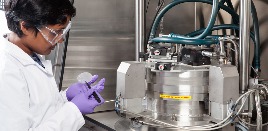
Much of our research is dependent on growing high quality single crystal (epitaxial thin films). We use a wide variety of techniques, including ultra-high vacuum sputtering for metals and metal heterostructure (for example Ho/Nb/Ho trilayers for superconducting spin valves (Gu PRL 2015), pulsed laser deposition for oxides (for example high temperature superconductors, colossal magnetoresistive materials and multi-ferroics, and metal-organic chemical vapour deposition (MOCVD) for nitride semiconductor devices (including light emitting diodes, high electron mobility transistors and single photon sources). To improve the properties and performance of the thin films and crystals we grow, we perform extensive characterisation using a range of techniques including X-ray diffraction, transmission electron microscopy and atomic force microscopy, and then feed back the results of these investigations to achieve improvements in the growth process.