All materials have surfaces and interfaces, and often these features control the properties of structures and components. For example, the interfaces of the multilayer stacks which make up the antireflection coatings on optics, or the thermal control barriers on windows. The surfaces of drill-tips, or of aero-engine turbine blades, are examples of some of the very highest specification components, developed through the precise optimisation of materials and their fabrication.
Layers and interfaces are studied through powerful modelling methods, leading to predictions for optimised thin film structures and coatings. Modern film deposition and growth techniques offer the capability to engineer surfaces down to the atomic scale. Combined with the highest resolution characterisation methods, surface properties such as hardness, reflectivity, and chemical stability, are being developed and tuned for a huge range of applications.
Capabilities in the Department include those for production of both thin (PVD & CVD) and thick (vacuum plasma spraying and plasma electrolytic oxidation) surface coatings, and also a suite of fine scale mechanical testing facilities (including 3 nanoindenters, one of which is housed in a vacuum chamber).
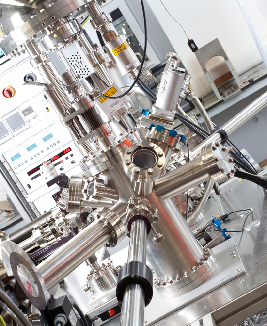
Figure caption: Ultra-high vacuum coating and surface analysis.