The development of new materials for Information and Communications Technologies (ICT) is fundamental to innovation, device performance, and energy efficiency for low-power (portable appliances) and high-power (data centre) applications. Research in the Department on materials for ICT is cross disciplinary and encompasses the development of devices for information processing and storage, and communication. Recent highlights are giant and reversible magnetocaloric effects in epitaxial ferromagnetic thin films, the discovery of spin-polarised supercurrents, transmission of electron spin information through carbon materials, scaled-up processing of gallium nitride light emitting diodes for visible light communications, control over the properties of functional oxide thin films, and world-leading developments in predicting material structure and properties from first-principle calculations.

Magnetoelectric effects arise when magnetic and electrical signals are interconverted. We study ferromagnetic films that experience voltage-driven strain from ferroelectric underlayers. The resulting magnetic changes are imaged using techniques such as magnetic force microscopy (MFM) – e.g. the left image shows magnetic domains in a manganite film (image diameter = 10 mm). We are also developing low-power, high-density, high-speed non-volatile magnetoelectric RAM. Currently, there is no single-phase material with a sizeable magnetoelectric effect at room temperature and so there are no practical devices. We are exploring new materials compositions or combinations to solve this problem by creating interface-coupled systems in superlattices and self-assembled nanocomposites.
Superconducting spintronics (Robinson)
Following our breakthrough in demonstrating spin-polarized supercurrents, we are Leading the world in understanding the coupling of magnetism and superconductivity to enable radical new methods of spin/charge coupling for future low energy computing technologies. Our vision is to combine these two technologies in order to develop the radically new field of “Supeconducting Spintronics”, which has the potential to eliminate size and heating constraints of memory/logic technologies based separately on superconductivity (RSFQ) and spintronics. Right photograph shows one of the Department’s state-of-the-art computer-controlled systems used for this research for sputtering metallic and insulating films with sub-nanometre thickness control.


The full exploitation of powerful modern computers requires the development of well designed, efficient and robust computer codes. Pickard is a leading developer of the CASTEP code, which uses density functional theory (DFT) to predict a wide range of materials properties. CASTEP (licensed to Biovia by the University of Cambridge) has been used by industry for over two decades and the UK research community has free access through the UKCP consortium. A new generation of computational scientists is being trained in the EPSRC Centre for Doctoral Training in Computational Methods for Materials Science, co-directed by Elliott. Left image shows a grain boundary structure in graphene predicted by DFT with armchair and zigzag regions.
Internet of things & visible light communication (Oliver)
Wireless data transfer is a normal part of everyday life, and the future promise of ever-more connectivity places ever-increasing demands on the available bandwidth for data-transfer. These demands are giving rise to new communication technologies, such as visible light communication, also known as LiFi, which exploits micro light emitting diodes (micro-LEDs) based on gallium nitride to transfer data at ultra-high speeds via high speed modulation of light intensity - which could mean an imperceptible flicker of your normal room lights, combining energy efficient lighting with data transfer. In collaboration with industry, the GaN Group are developing the materials and technologies to render this new technology manufacturable at the large scale, and are installing Veeco MOCVD systems for high throughput production on large area wafers.

Quantum light sources (Oliver)

Light sources which emit a controlled number of photons on demand, either a single photon or a pair of entangled photons, have the potential to revolutionise future computing and communications. Their possible applications range from providing a source of genuinely random numbers for conventional computers to enabling perfectly secure data transfer via quantum key distribution for cryptography. They could allow the development of ultra-parallel computing: linear optical quantum computation. Whilst the first single photon emitters developed in Cambridge operated at a few degrees above absolute zero, engineering the materials from which they are made has allowed us to develop devices operating at temperatures accessible by on-chip cooling, bringing practical application of this quantum technology a step-closer to reality. Left image shows part of an array of GaN-based single photon sources.
Graphene spintronics (Mathur)
The ability to send spin-polarized electrons through a non-magnetic channel running between ferromagnetic electrodes could be exploited in future logic and memory devices. Having previously shown that a carbon nanotube can carry spin-polarized electrons without significant depolarization, we have now done likewise with graphene. An important step on the journey was to perfect magnetic switching in highly spin-polarized manganite electrodes. The image below shows a magnetic image of this good switching, obtained in collaboration with Sarnjeet Dhesi at Diamond Light Source.

New forms of non-volatile RAM and cognitive computing (Driscoll)
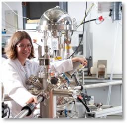
There are emerging non-volatile RAM technologies that offer the promise of faster, higher density, lower energy memory than is currently possible. Oxide resistive RAM is one technology, but there are challenges of reproducibility and endurance. This is because electronic and ionic processes are coupled and the resistive channels in the devices form randomly at defect sites. We are exploring nanoengineered structures where ionic and electronic channels are separated, and which offer tuneable on-off ratios, endurance and reproducibility. This research includes investigating ‘neuromorphic’ cognitive computing and ‘in-memory’ logic, for new non-von Neumann computing. Right photograph shows a recently setup state-of-the-art pulse laser deposition system in the Department for layer-by-layer growth of oxides thin films.
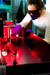
Nanospectroscopy (Di Martino)
Nanoscale materials investigation and manipulation is a crucial need of a society experiencing constant scaling down of devices footprint and proliferation of innovative materials by nano-engineering. We link the fields of nanoscale materials engineering and plasmon-enhanced light-matter interactions so as to explore the real-time changes in materials behaviours within 3D nanoscale active devices with inexpensive, non-destructive and at the same time fast and accurate spectroscopy techniques able to give the necessary feedback to direct materials engineers towards a systematic development of very fine (atomic-nanoscale) structures, as well as to enable light induced materials manipulation. The photograph shows a recently setup state-of-the-art plasmon enhanced spectroscopy system in the Department for in-situ and real-time investigation of oxides thin films devices.