
Professor of Materials Physics
(jointly appointed with the Cavendish Laboratory)
BSc Imperial College London
MSc Imperial College London
PhD Imperial College London
My research focuses on the development of advanced, high efficiency III-V photovoltaics. The PV market for domestic electricity is extremely cost sensitive and as such is dominated by Silicon solar cells, which now enable cost parity with grid electricity in many parts of the world. Silicon technologies, however, are not so well suited to applications including powering satellites, space exploration and unmanned vehicles where efficiency, radiation tolerance, weight and form factor are also critically important. Many aspects of modern life including agriculture, defense, emergency services and individual mobile connectivity are dependent on these systems to provide ubiquitous functionalities such as communications, navigation, precision timing, meteorological data and real-time imaging. My research seeks to develop novel materials and device architectures to power these systems.
Ultra-thin III-V photovoltaics
Ultra-thin (<200 nm) III-V photovoltaics are an emerging device concept, to increase W/kg while also enabling new fully flexible satellite form factors. This technology offers intrinsic radiation tolerance, to enable extended missions in challenging space environments such as polar earth orbits and Jovian exploration. Traditional PV devices are usually several microns thick. This is required for full absorption of incident solar illumination however, it also means that photo-generated charge carriers have a longer distance to travel before they can be collected at the device terminals. In space environments photovoltaic devices are bombarded with high energy charged particles which introduce defects into the absorbing semiconductor material, severely degrading device performance. Charge carriers are much more readily extracted in ultra-thin devices making them less sensitive to the presence of defects and therefore better able to survive radiation exposure. In order to fully absorb incident solar illumination in an ultra-thin semiconductor film, advanced light management approaches are required such as the use of sub-wavelength nanophotonic scattering structures to couple light into laterally propagating modes. In this way, a device which is optically thick but electrically thin can be fabricated.
Development and characterization of novel III-V alloys
As optoelectronic devices evolve, novel III-V multi-species alloys are increasingly employed to engineer the combination of bandgaps and band alignments necessary to manipulate carrier dynamics and achieve new functionality and high performance. In practice, the growth of these alloys can be extremely challenging because the immiscibility of certain compositions can lead to phase segregation within the solid, which severely degrades the material's optical and electronic properties. Luminescence characterisation methods including temperature and power dependent photoluminescence as well as nanoscale imaging techniques such as scanning transmission electron microscopy are critical to understanding these novel materials and effects of composition, growth temperature and annealing on their material properties. As well as performing characterisation, my research seeks to develop computational tools to provide a quantitative interpretation of the results.
Advanced photovoltaics concepts with III-V quantum well structures
The material properties of III-V alloys can be further engineered using quantum confining structures for new device functionality. The hot-carrier solar solar is fundamentally different type of solar heat engine, which can exploit the properties of quantum well structures, in theory enabling solar energy conversion efficiencies up to 85%. This is achieved by preventing the dissipation of photon energy above the bandgap of the absorber as heat in the lattice and extracting carriers from the device whilst they are still “hot”. My research is this area focuses on the characterisation of carrier dynamics in III-V quantum well structures to develop materials which exhibit restricted carrier-phonon interaction. By adjusting alloy composition of barrier and well materials, electron and hole confining potentials can be independently tuned allowing for interaction rates to be engineered. This concept is well established within the field of quantum cascade lasers, however my research demonstrates that these systems are also promising candidates for hot-carrier solar cell development.
|
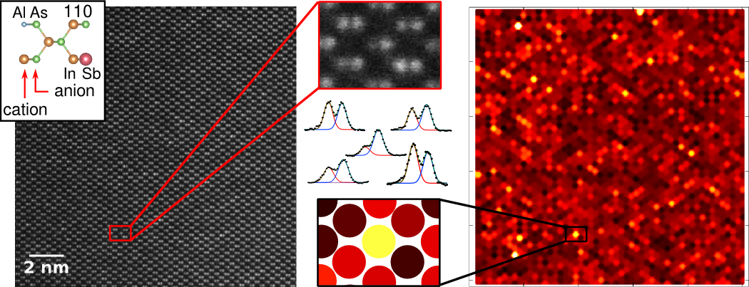
Quantification of a high resolution scanning transmission electron microscope image of the novel alloy InAlAsSb showing relative anion and cation atomic column contrast. |
 |
-
L. C. Hirst, N. A. Kotulak, S. Tomasulo, J. Abell, M. González, M. K. Yakes, J. R. Meyer, R. J. Walters, C. Song, P. Specht, P. Ercius and C. Kisielowski. “Imaging atomic scale clustering in III-V semiconductor alloys”, ACS nano (2017)
-
L. C. Hirst, M. K. Yakes, J. H. Warner, M. F. Bennett, K. J. Schmieder, R. J. Walters, and P. P. Jenkins. “Intrinsic radiation tolerance of ultra-thin GaAs solar cells” Appl. Phys. Lett. 109(3): 033908 (2016)
-
L. C. Hirst, M. P. Lumb, J. Abell, C. T. Ellis, J. G. Tischler, I. Vurgaftman, J. R. Meyer, R. J. Walters, M. González. “Spatially indirect radiative recombination in InAlAsSb grown lattice-matched to InP by molecular beam epitaxy” J. Appl. Phys. 117(21):215704 (2015)
-
L. C. Hirst, R. J. Walters, M. F. Führer, N. J. Ekins-Daukes. “Experimental demonstration of hot-carrier photo-current in an InGaAs quantum well solar cell” Appl. Phys. Lett. 104(23):231115 (2014)
-
L. C. Hirst, H. Fujii, Y. Wang, M. Sugiyama, N. J. Ekins-Daukes. “Hot carriers in quantum wells for photovoltaic efficiency enhancement” IEEE J. Photovolt. 4(1):244-252 (2014)
-
L. C. Hirst, N. J. Ekins-Daukes, “Fundamental losses in solar cells” Prog. Photovolt. 9(3):286-293 (2011)