As the global demand for electricity continues to surge, the efficiency of switching systems becomes increasingly paramount. GaN-based high electron mobility transistors (HEMTs) exhibit excellent electrical characteristics such as high breakdown voltages, low on-resistances, and fast switching, making them promising for power switching applications like electric power transmission, electric vehicles, and solar inverters, among others. By minimising wasted energy, they help reduce operational costs and contribute to the reduction of greenhouse gas emissions, thereby playing a crucial role in creating a more sustainable future. Recently, the lateral dimensions of GaN-based HEMTs have been reduced to the sub-100 nm scale. Therefore, it is critical to understand the local electrical properties near the HEMT surface with nanoscale resolution.
In this paper, we used scanning capacitance microscopy (SCM), an atomic force microscopy (AFM)-based technique that employs a nanoscale conductive tip to characterise the HEMT surface. We developed the methodology for SCM plan-view characterisation of GaN-based transistor structures by systematically investigating the impact of imaging conditions and the experimental setup on the SCM contrast observed in the HEMT structures measured in plan view. Based on this, we found that nanoscale surface defects in GaN-based HEMTs can change local electrical properties. Additionally, the inhomogeneity of the epitaxial layer in terms of layer thickness and composition can also lead to local variations in electrical properties. This study provides a foundation for exploring structure–property relationships in GaN-based HEMT structures. The methodology could potentially find application in other types of HEMT structures, such as GaAs-based HEMT structures, and other highly-doped samples.
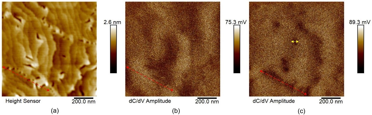
Figure caption: (a) Topographical, and (b) and (c) SCM amplitude data for the same area on a GaN-based HEMT structure, captured at two optimised DC biases. SCM amplitude is linked to the local carrier concentration. The red lines indicate the same position. The contrast in defective regions demonstrates that defects alter local electrical properties. In non-defective regions, the contrast also indicates sub-surface inhomogeneity in layer thickness or alloy composition. The yellow arrow in (c) highlights a feature with a width of about 60 nm, demonstrating the nanoscale resolution of the technique.
Chen Chen, Saptarsi Ghosh, Francesca Adams, Menno J. Kappers, David J. Wallis, and Rachel A. Oliver, "Scanning capacitance microscopy of GaN-based high electron mobility transistor structures: A practical guide.", Ultramicroscopy 254 (2023): 113833