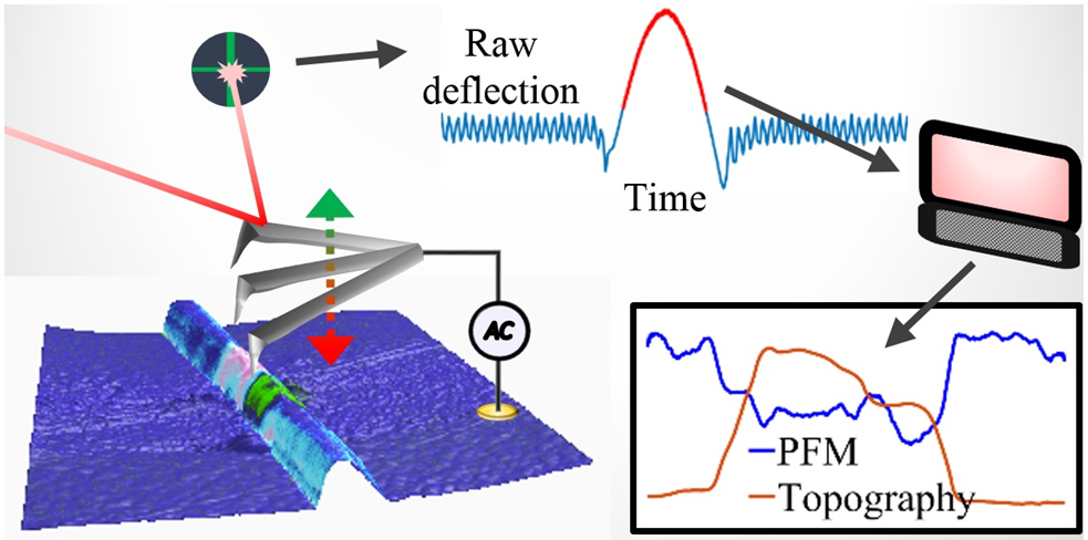
There has been tremendous interest in piezoelectricity at the nanoscale, for example in nanowires and nanofibers where piezoelectric properties may be enhanced or controllably tuned, thus necessitating robust characterization techniques of piezoelectric response in nanomaterials. Piezo-response force microscopy (PFM) is a well-established scanning probe technique routinely used to image piezoelectric/ferroelectric domains in thin films, however, its applicability to nanoscale objects is limited due to the requirement for physical contact with an atomic force microscope (AFM) tip that may cause dislocation or damage, particularly to soft materials, during scanning. Here we report a non-destructive PFM (ND-PFM) technique wherein the tip is oscillated into “discontinuous” contact during scanning, while applying an AC bias between tip and sample and extracting the piezoelectric response for each contact point by monitoring the resulting localized deformation at the AC frequency. ND-PFM is successfully applied to soft polymeric (poly-L-lactic acid) nanowires, as well as hard ceramic (barium zirconate titanate–barium calcium titanate) nanowires, both previously inaccessible by conventional PFM. Our ND-PFM technique is versatile and compatible with commercial AFMs, and can be used to correlate piezoelectric properties of nanomaterials with their microstructural features thus overcoming key characterisation challenges in the field.
Figure: A non-destructive piezo-response force microscopy (PFM) technique is presented for mapping piezoelectricity in nanoscale systems previously inaccessible by conventional PFM.
Y. Calahorra, M.Smith, A. Datta, H. Benisty and S. Kar-Narayan, “Mapping piezoelectric response in nanomaterials using a non-destructive scanning probe technique”, Nanoscale (2017)